Color : blue
Density at 20°C: 0.87 g/cm
3 Drying time at 70°С: 15 min
Flow rate: 15 m
2/liter
Photosensitivity: 310-440 nm
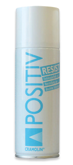
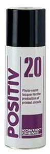
Purpose: POSITIV 20 - a photosensitive varnish used by both technical specialists and non-professionals in the small-scale production of printed circuit boards, copper engravings and when carrying out work related to the transfer of images to various materials.
Properties: High exposure characteristics provide good contrast of transferred images.
Packing: in aerosol cans 100ml., 200ml.
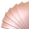
Modern production of electronic equipment is inconceivable without the use of printed circuit boards, in the production of which the technique using photo-varnishes is one of the main ones. This applies equally to industrial production and to piece production of prototype boards or small batches that are designed and manufactured daily for the electronics industry. For these purposes, it was important to develop a photolacquer that meets the following requirements:
- ease of use;
- always ready to use;
- easy to remove and at the same time resistant to pickling acids;
- high exposure properties;
- low production costs
All of these qualities are fully consistent with the photoresist varnish
POSITIV 20. Forget about all the problems you faced in the past in the manufacture of printed circuit boards. Using the tool
POSITIV 20 in the manufacture of boards simplifies the process of their manufacture to the level of child's play. From
POSITIV 20 the exposure of the image is made directly from the positive without intermediate production of negative images, and after development you get a high-quality contrasting image of the tracks, which gives all the advantages of copy perfection. The procedure itself is not complicated, practical and relatively inexpensive when preparing piece and small-scale products. A 200 ml aerosol can is usually enough to cover 4m2 of copper.
Some catalogs publish drawings of printed circuit boards in 1: 1 scale. By means of an aerosol-transporting agent with a stamp
¦
¦
TRANSPARENT 21 , you can make such schemes transparent to light and transparent to ultraviolet radiation. Thus, it becomes possible to directly copy board designs directly from catalog pages onto surfaces treated with the composition
POSITIV 20.
After cleaning, to effectively protect the surface from the formation of oxides and simplify the soldering process, we recommend treating the board with -
¦
¦
FLUX SK 10.
After carrying out soldering work on the boards you have made, to protect against environmental influences (moisture penetration between the tracks, insects, etc.), we recommend that you carry out a protective treatment with a agent
¦
¦
PLASTIK 70.
¦
¦
PLASTIK 70 is a varnish based on acrylic rubber that, after spraying on the surface of the boards, forms a transparent film with high dielectric properties and high resistance to aggressive media. It is also important that this type of protective film allows subsequent soldering of metal surfaces.
INSTRUCTIONS 1. Pre-treatment - surface cleaning. The surface on which the photoresist will be applied must be absolutely clean and dry.
2. Application. To use the photoresist
POSITIV 20 there is no need for a dark room, since in the liquid state the photoresist is insensitive to light, but the work should be carried out in diffused light, excluding the possibility of direct exposure to the solar surface rays or close proximity to the work site of sources of bright illumination. Also, it is very important that there is no air movement in the room where the work is carried out. The photoresist should be applied at room temperature.
Spray from a distance of approximately 20 cm. Spray the aerosol in continuous zigzag strokes starting from the top left corner to create a uniform coating. Do not use an excessive amount of aerosol, as this leads to the formation of unwanted smudges and the formation of a non-uniform coating thickness, requiring a longer exposure time (see point 5). Once the coating is finished, the boards should no longer be exposed to light.
The color of the coating gives an approximate estimate of the thickness of the resulting layer:
light gray - blue: 1 - 3 microns dark gray - blue: 3 - 6 microns blue: 6 - 8 microns dark blue: more than 8 microns Copper coating may have a greenish tint. After cleaning with detergent, rinse the board with plenty of water to remove any residue and abrasive inclusions. After rinsing, do not let the surface come into contact with any other solvents (such as acetone, alcohol). The plates must be dried between sheets of absorbent paper. Photolacquer should be applied immediately after cleaning the surface in order to avoid the appearance of an oxide film.
3. Drying After spraying the composition, the boards should be immediately transferred to dry in a dark place. Drying is performed to remove solvent elements from the coating. The degree of light sensitivity of the coating increases during the drying process. Boards coated with photoresist varnish can be dried at room temperature for 24 hours. You can speed up drying in an oven or oven controlled by a thermostat at 70°C for 20 minutes.
Stock of dried boards should be stored in a cool and dark place.
4. The original layout. Use ink and transparent paper/film with a density of 90 g/m2 to draw images of printed circuit boards. The film must allow the penetration of ultraviolet rays (in no case should it have a yellow tint). It is recommended in the presence of especially small details - drawing of narrow and closely spaced tracks to place the film with a drawing to the board. It is recommended to apply ink drawing on a completely dry base to eliminate smudges and reduce contrast. For best results, you can add a little yellow color to the mascara, which prevents the penetration of UV rays.
If you have a personal computer, you can design a negative of a printed circuit board using specialized software (for example, PCAD) and print on a laser or inkjet printer. In this case, you can print the image not on paper, but immediately on
¦
¦
special transparencies for laser printers or
¦
"
for inkjet printers .
A computer-printed image of the board on film allows for finer spacing and high board quality.
5. Exposure Photoresist varnish
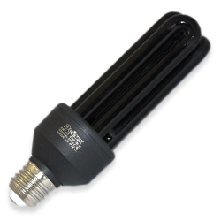
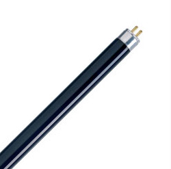
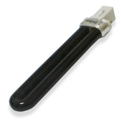
POSITIV 20 is sensitive to ultraviolet rays, so you can use, for example, a Philips HPR 125W mercury lamp or 300W quartz lamps. The best results are obtained with ultraviolet radiation with a wavelength of 360-410nm. Sufficiently satisfactory results were obtained using an ordinary 200W incandescent lamp as a light source with exposure from a distance of 12 cm. A good exposure result is achieved with domestically produced fluorescent lamps such as LD-18, LD-20 (for these lamps, the exposure time is 5-10 minutes). Recently, "energy-saving" fluorescent UV lamps with a standard E27 base have appeared, namely
¦
¦
EBT-01.
Do not start illumination until the stability of the light source is obtained, it is necessary for the lamp to warm up for 2-3 minutes. The exposure time depends on the thickness of the coating and is usually 60-120 seconds when the light source is located at a distance of 25-30 cm. Glass plates used during exposure can absorb up to 65% of ultraviolet radiation.
Therefore, in such cases, it is necessary to increase exposure time. The best results are obtained when using plexiglass plates. When using a photoresist layer with a long shelf life for the application, the exposure time can be doubled.
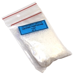
6. Development. Development of already exposed boards can be performed in diffused daylight. Developer preparation: add
¦
¦
8 grams of caustic soda (NaOH) to one liter of cold water. For properly exposed surfaces on 4-6 micron photoresist layers, the development time in a fresh solution is usually 30-60 seconds and does not exceed 2 minutes. The temperature of the solution should be in the range of 20-25°C. If the exposure was excessive, or the ink used to make the drawing was not opaque, the image of the conductive paths will appear for a while, but will eventually be removed by the developer.
7. Etching. Photoresist varnish
POSITIV 20 resistant to acid solutions containing ferric chloride - Fe3Cl, ammonium persulfate - (NH4) 2S2O8, hydrochloric and hydrofluoric acid.
For etching copper plates, an iron chloride solution is recommended at an operating temperature of approximately 45°C and a concentration of 35-40% for 30-60 minutes. Stir the solution slightly to speed up etching. For fast etching, the practice of using a mixture of the following composition has become widespread:
200 ml of hydrochloric acid (HCl - 35%) 30 ml of hydrogen oxide (H2O2 - 30%) 770 ml water (H2O) Etching time approx. 10 min. Regeneration of the solution with increasing etching time of subsequent boards is carried out by adding hydrogen oxide. This mixture has a pungent odor and slight fumes. Therefore, work with it is done with great care. Avoid contact with skin, but if this happens, the contact area must be thoroughly rinsed immediately. Wear safety goggles and clothing when handling solvent.
8. Final cleaning. After etching and rinsing the boards, a final cleaning should be carried out, for example: with acetone.


 The data presented in the product description are for reference only and may differ from those indicated by the manufacturer.